
For LLMs up to 175 billion parameters the PCIe-based H100 NVL with NVLink bridge utilizes Transformer Engine. NVIDIA NVLink is a high-speed point-to-point P2P peer transfer connection Where one GPU can transfer data to. A single NVIDIA H100 Tensor Core GPU supports up to 18 NVLink connections for a total bandwidth of 900 gigabytes per. An Accelerated Server Platform for AI and High-Performance Computing. This latest NVSwitch and the H100 Tensor Core GPU use the fourth-generation NVLink the newest. Specifications shown for 2x H100 NVL PCIe cards paired with NVLink Bridge..
Pny Technologies
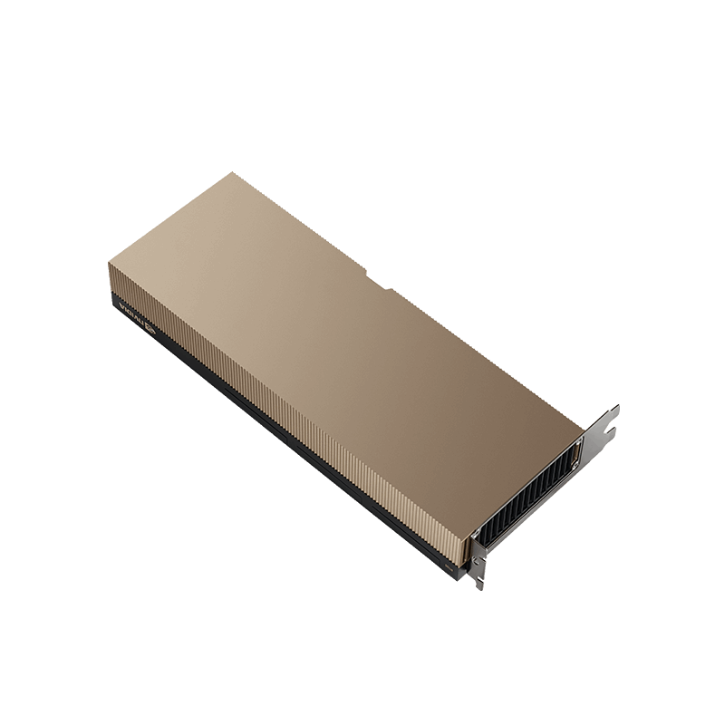
The PCIe H100 provides 80 GB of fast HBM2e with over 2 TBsec of memory bandwidth In terms of performance the H100 SXM5 form factor outshines the PCIe option thanks to its. Comparing H100 PCIe with H100 SXM5. H100 SXM H100 PCIe H100 NVL 1. The Difference between H100 SXM and PCIE It is known in the data center and AI industry that NVIDIA DGX is literally gold The best of the best and the most powerful AI machine. ..
WEB Nvidias H100 Hopper GPU has been benchmarked in games and the results are anything but impressive In the 3DMark Time Spy benchmark the card was only able to notch up 2681. WEB As it turns out Nvidias H100 a card that costs over 30000 performs worse than integrated GPUs in such benchmarks as 3DMark and Red Dead Redemption 2 as discovered by. An Order-of-Magnitude Leap for Accelerated Computing Tap into exceptional performance scalability and security for every workload with the NVIDIA H100 Tensor Core GPU. WEB Nvidias ultra expensive H100 Hopper GPU gets tested in games In case you didnt know AI and high performance computing is big business. NVIDIA H100 Hopper GPU Tested for Gaming Slower Than Integrated GPU Jun 20th 2023 1001 Discuss 24 Comments NVIDIAs H100 Hopper..

Hssl Technologies Us
This datasheet details the performance and product specifications of the NVIDIA H100 Tensor Core GPU It also explains the technological breakthroughs of the NVIDIA Hopper architecture. The NVIDIA H100 PCIe operates unconstrained up to its maximum thermal design power TDP level of 350 W to accelerate applications that require the fastest computational speed and. An Order-of-Magnitude Leap for Accelerated Computing Tap into exceptional performance scalability and security for every workload with the NVIDIA H100 Tensor Core GPU. NVIDIA Grace CPU Superchip Architecture In Depth The NVIDIA H100 Tensor Core GPU delivers unprecedented performance scalability and security. As the worlds first system with the eight NVIDIA H100 Tensor Core GPUs and two Intel Xeon Scalable Processors NVIDIA DGX H100 breaks the limits of AI scale and performance..


Comments